please tell me - exactly who - what market - is able to afford these ?
https://www.serversupply.com/SSD/NVMe/122.88TB/SOLIDIGM/SBFPF2BV0P12OP1_407563.htm
At $12,750 for ONE drive - who can afford to buy 12 or 24 of these ?
bob
please tell me - exactly who - what market - is able to afford these ?
https://www.serversupply.com/SSD/NVMe/122.88TB/SOLIDIGM/SBFPF2BV0P12OP1_407563.htm
At $12,750 for ONE drive - who can afford to buy 12 or 24 of these ?
bob
Flash memory storage (NVMe or SATA based) seems to be stuck for years now.
Unless controller makers are deliberately keeping the max capacity down, I don’t see a reason (I have seen DRAM cost limitations mentioned, but that can’t be it), why consumers cannot buy reasonable priced SSD storage.above 2TB
Look at how much space SATA storage actually uses up in 2.5 inch casings
I asked WD reps at a QNAP Vancouver event 2 years ago and all they had was shrugs
Because they can.
you boys ain’t answering the question. I didn’t ask WHY it’s so expensive - I asked WHO are the clients that are spending this kind of money. I work for some huge corporations with massive budgets, and they WILL NOT spend this kind of money for storage.
Only thing I could think of is AI companies, they have the buzzword investor cash, that is the money printing machine these days. (The same as crypto coins were a decade ago).
Maybe their data models need to be shuffled in and out of the dedicated NVIDIA AI cards, as fast as possible and no amount of money is too much
Sometimes, it’s just done as a showpiece with not a lot of plans to actually sell many. For those who want it - they have it. I’m sure someone is buying it and paying that price.
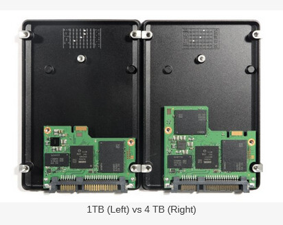
I would suspect that a 128TB drive takes up a bit more space inside the housing than what Dolbyman shows.
I sell for one of the 5 top manufactures of micro-controllers and micro-processors. We also sell NOR flash. NOR flash is limited to a 40 nm process. I’m not sure about NAND flash*. What that means is that while processors are being built at process nodes like 22 nm or even smaller (heck - I think some of the new Apple M chips are on like 1 or 2 nm process nodes), flash is kinda stuck where it’s at. You can do other styles of memory like MRAM which can go down to at least 22 nm but it’s much more expensive than flash and has limitations around strong magnetic fields. Chip size is directly related to process node size. So you can only get so much density for an area of silicon at 40 nm. The more higher memory density you want then, the larger the chip becomes. In our MCUs, the single most “expensive” area of the chip that takes the most space on the die is the RAM. The second most expensive area is the flash space.
Larger density chips get more expensive and you then need the circuitry and so forth to bridge the chips together. I don’t know if that justifies a $12K price tag for a 128TB flash drive. But this die size limitation due to process node size is probably the reason the technology has kind of plateaued.
*All mass storage products use NAND flash. NOR flash is typically used to handle things like firmware and application code in a device. I am not as familiar with NAND flash and if NAND flash is limited to certain process node sizes. I suspect it is.
Well that article answers the original question: “AI training Center” And they can certainly afford it!